
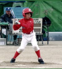
Katsyua in his childhood at a local festival in Japan.

Published: | By: Ira Winkler
Katsuya came to us for his Master's degree in Photonics and stayed for his doctorate. What drives him and how much he has achieved until now is inspiring.
Katsuya, many colleagues have no idea about life and culture in Japan. For this reason, it is exciting to learn from you, for example, about the world you come from and what motivated you to come to Jena. The more we learn about each other, the more we recognise similarities and are no longer strangers. So I have a few questions for you:


Can you briefly describe how you grew up? Was science a topic in your family? What was particularly important in your education, both at home and at school?
I grew up in Fujiidera city in Osaka prefecture in Japan. My home was surrounded by vast rice paddies and lush vegetable fields. My family name “Tanaka” means “center of the rice fields” which actually is named after my ancestor’s occupation working in rice fields. Apparently, for my family, we have a tradition of inheriting the rice fields over many generations (probably longer than hundreds of years) and, of course, my grandparents wanted me to take over all our farming lands and I learned all the agricultural techniques from my family. When I was an elementary school student, I wanted to be a professional baseball player and started playing baseball since I was 8 years old. I actively enjoyed playing baseball till I was 17. But, gradually, my dream was shifting to becoming an ”inventor” through my elementary school and junior high school educations. I remember that I got so much into a summer science project from my elementary school. I got a prize for crafting a small model of locomotive, which runs with a compact-sized steam engine. After that, I started getting stronger curiosity in science and engineering. With my dad’s support, I crafted many things like a small LEGO robot fully automated with an external program, a metal detector, radio system, hydrometer, a lie detector with electric circuit builders. My dad was a technology and science teacher in a local junior high school. So I was so lucky that I could enjoy learning a lot from him about these subjects. However, during weekends, when he took me to the farmlands, unfortunately I couldn’t enjoy doing a lot of agricultural tasks because I felt so bored of doing repetitive chores. As I entered high school, I experienced a sudden loss of motivation for studying that persisted for two years. This is because I wasn’t sure what I want to be and also I kinda didn’t like the ideas about “studying for enrolling into a good University”. But one day one physics teacher at the high school triggered me. He explained a concept of wave-particle duality of light. I felt that this physics is very deep! Since then I studied physics and math with a lot of fun, (and also English with my mom’s help because she was an English teacher) and ended up locating myself in Hamamatsu, which is the most famous photonics city in Japan, for my bachelor program. This city is called “photon valley” and is very famous in photonics industries and education. I was very happy to participate in the course of opto-electronics and precision engineering, mechanical department, faculty of engineering, in Shizuoka University.
So you were enthusiastic about interesting physics projects and theories. Were there any other events or phenomena that pointed you in the direction of photonics?
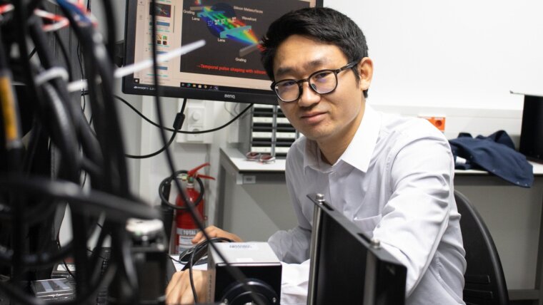
During my Bachelor program, I have taken not only fundamental physics and mathematics courses but also mechanical engineering, electrical engineering and experimental and theoretical photonics courses. I took many photonics-related courses in the third year of my Bachelor degree. Through one of these courses I became very curious about one physics phenomenon on light-matter interaction at metal-dielectric interface. That triggered my curiosity in deepening this field, especially understanding mathematically light propagation at metal-dielectric interface. I started questioning myself why this happens, under which conditions, and how useful it is in reality. I found it interesting that very unnatural behaviors of light can happen on nanoscale. Afterwards to understand this further, I started my research in the field of nanophotonics in Prof. Kawata’s group and additionally learned various topics of photonics in his group such as laser trapping technologies, ultrahigh-resolution microscopy, ultraviolet lithography techniques, holography generation and so on. That is the time when I felt that “photonics is the future”.
On the other hand, it seemed that my family wanted me to come back to Osaka after my Bachelor’s degree to take care of the faming fields as a side job. But I managed to convince them that I wanted to fully focus on becoming an expert in photonics with my passion.
How did you find out about the opportunities in Germany or here in Jena and were there any hurdles on the way here?
My experience in Nebraska in the US as a short exchange program during my undergraduate changed me a lot. I had a chance to travel to Nebraska state in the US for a summer international exchange program, which expanded my horizon completely. I could imagine many possibilities outside of Japan. The world is very wide and there are so many things I don’t know. I became passionate about learning new culture and getting to know new people from different countries. Therefore, I was very active meeting foreign students at Shizuoka University. I was a part of organizing team of English Speaking Society for international students at Hamamatsu Campus in Shizuoka University. Through my active commitment to international activities, accidentally I met two German students from Jena. The reason is that Shizuoka University has a long-term collaboration partner in Fachhochschule Jena and every year they exchange one or two students every year. I instantly became friends with them and asked tons of questions about Jena. Then I learned that Jena is a global leading photonics city and they explained how amazing facilities in photonics Jena has. Also I learned that there is an fully English-taught photonics program. Then I set a goal to first enroll in the Abbe School of Photonics master Program in Jena and establish a bridge between Hamamatsu and Jena because they are both world-wide famous photonics city. But it wasn’t an easy process because I learned science and math all in Japanese for my entire life back then and had to be prepared for all the English education in photonics. So I read a book called “Fundamentals of Photonics” all in English and learned a lot of scientific vocabularies in English, wrote my Bachelor thesis in English, and did the bachelor defense in English. In Japan, doing something different from others require a lot of courage. Usually many people in Japan feel comfortable doing the same as others. But my motivation was unstoppable back then, and was already preparing for non-Japanese mindset to prepare for studying abroad, which was also needed to adapt to different international communities.
Oh, that shows a strong will and great curiosity! What helped you the most when you arrived here in this foreign culture and what do you miss most? What was the biggest surprise for you here in Jena? How has your experience as a doctoral student in Germany been so far? Were there any particular challenges or highlights that you would like to share?
I became friends with my classmates nicely here and my friends from the master program were really precious to me. I struggled understanding direct expressions because Japanese people are so indirect when speaking. Many Germans around me were so direct to me for anything like even something very critical! I felt so shocked at the beginning. But many of my classmates gave me some tips to overcome such a cultural difference and they were very nice to me all the time. My classmates during my master program in Abbe School of Photonics are really my treasure. But it was still very hard to integrate myself to German communities outside of the international master program and PhD program. So eventually I started establishing a local Japanese-German mixed community together with Japanese people and German people learning Japanese, called Japanstammtisch Jena. I think that in Japanese culture, belonging to a community is very important because we feel secure in harmony in group and we are inter-dependent on each other compared to many other culture. Through this community I could easily meet other Japanese living in Jena who can share the similar feeling and experience and also meet Germans who are interested in understanding our culture. This community game me a lot of happy feeling to me.
Of course, I missed a lot my rice and vegetables from my farmlands and also my family in Japan. But I go back to my hometown every year and meet my family, eat a lot of Japanese food, and also help my dad’s agricultural works.
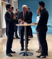
Respect for what you have achieved here in terms of integration - thank you for enriching Jena in this way! You also just had the opportunity to speak with the Federal President and the Prime Minister of Thuringia - what impression did you take away from this meeting? What questions would you have liked to ask?
Well, he was so friendly and so easy to talk to. We talked about why we came to Jena and what we want to do in our future. He seemed to be impressed that this city Jena attract many international students. Also He asked us how integrated we are in Germany and our German level. We switched to speaking in German at some point and we somehow managed to hold our conversation in German. I wanted to ask some critical questions such as German beurocracy, public transport, apartment finding for foreigners and so on. But we didn’t have enough time to cover many topics.
These are certainly issues that concern many of us. What are your future plans after completing your doctoral studies? Are there any particular topics you would like to focus on or what would you like to achieve here in Jena or Germany - perhaps in your home country or for the future in general?
After finishing my PhD, I would like to still contribute to the collaboration between Jena and Hamamatsu. Through my educations, I really got both academic and industrial connections in Hamamatsu and Jena. I recently organized the Jena-Hamamatsu photonics symposium 2024, which involved many people from both cities and it was a great trigger for fostering our ongoing international collaborations and student exchange. I think there are more things that I can do with this collaboration. So I think Jena gives the best opportunities to achieve my goal.
I am convinced of that! So you can recommend studying or doing a doctorate here at the university to others, what tips would you give?
I can recommend doing a PhD here especially to the people who want to establish a career in photonics. There are so many state-of-the-art technologies in photonics in Jena. At Beutenberg Campus, there are institutes that are very collaborative and supportive. So we can share high-tech devices, setups, and programs and so on. Also there are many photonics industries in Jena and nearby. So if you want to transition to industry later, there are bunch of options available for you.
Thank you so much for your inspiration and good luck for your future plans!